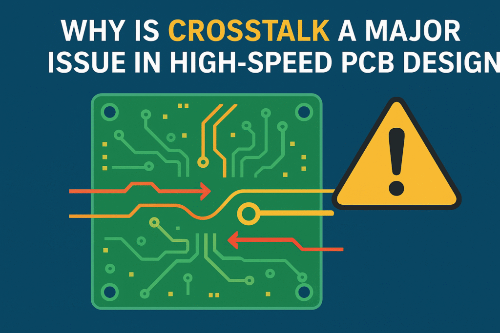
In the world of modern electronics, precision and reliability are essential for every circuit design. As electronic devices become faster and more compact, the need for high-performance circuit boards has never been greater. However, with speed comes complexity, and one of the most critical challenges faced by engineers offering PCB design services is mitigating crosstalk in high-speed PCB layouts. Crosstalk unwanted interference between signal traces can significantly affect signal integrity, causing data errors, timing failures, and unpredictable performance.
This article explores why crosstalk has become a major issue in high-speed PCB design, the science behind it, its impact on performance, and proven layout strategies that engineers can use to manage and prevent it based on the latest industry standards and Google’s 2025 content quality norms.
Understanding Crosstalk in PCB Design
Crosstalk occurs when an electromagnetic field generated by one signal trace couples into an adjacent trace, inducing unwanted noise or interference. This phenomenon becomes particularly noticeable in high-speed PCB design, where signal rise times are extremely short, and frequencies are high. In simpler terms, when two or more signal paths run too close to each other, one can “talk” to the other hence the name crosstalk.
There are two primary types of crosstalk:
- Near-End Crosstalk (NEXT): Interference measured at the same end as the signal source.
- Far-End Crosstalk (FEXT): Interference that appears at the receiving end of the trace.
Both types can distort signals, reduce timing margins, and even cause complete communication failures in high-speed circuits.
Why Crosstalk Matters More in High-Speed PCB Design
As technology advances, devices rely heavily on high-speed communication between components. With the introduction of multi-gigabit data transfer rates, reduced trace spacing, and complex layer stack-ups, the potential for crosstalk has grown exponentially.
Here’s why it’s a critical concern:
- Reduced Noise Margins: Faster switching signals leave less tolerance for interference, making circuits more sensitive to even minor noise.
- Miniaturization of Components: Compact board layouts force traces to be closer together, increasing coupling effects.
- Increased Signal Density: More high-speed signals running parallel raise the likelihood of electromagnetic interference.
- Higher Operating Frequencies: As frequencies rise, so do the capacitive and inductive coupling effects between traces.
These combined factors make crosstalk not just a minor nuisance but a major design challenge that can compromise functionality and long-term reliability.
Root Causes of Crosstalk in High-Speed PCBs
Crosstalk typically arises from poor trace layout or incorrect stack-up configuration. Some common causes include:
- Parallel Routing: Long parallel traces increase electromagnetic coupling.
- Inadequate Ground Reference: Poor grounding and return path design amplify noise.
- Improper Layer Stack-up: Insufficient isolation between signal layers enhances coupling effects.
- Uncontrolled Impedance: Variations in impedance lead to signal reflections that worsen interference.
- High-Speed Edge Rates: The faster the signal transition, the higher the risk of crosstalk.
By understanding these root causes, designers can take preventive measures early in the design process to maintain performance and reliability.
Impact of Crosstalk on PCB Performance
The effect of crosstalk on PCB performance can range from mild disturbances to complete signal distortion. In high-speed applications such as data communication, industrial automation, and computing systems, crosstalk can lead to:
- Signal Timing Errors: Unwanted noise causes jitter or delay in data signals.
- Bit Errors: Distorted signals lead to incorrect data transmission.
- Reduced Signal-to-Noise Ratio (SNR): Lower SNR decreases communication reliability.
- Increased Power Consumption: Repeated retransmissions to correct data errors consume more power.
- EMI Compliance Issues: Excessive coupling can lead to electromagnetic interference violations.
When these problems occur in mass-produced electronics, they can translate into costly redesigns, reduced product lifespan, and customer dissatisfaction.
Design-Level Strategies to Minimize Crosstalk
Modern PCB design services employ a combination of layout optimization, signal integrity analysis, and simulation tools to mitigate crosstalk. Here are some proven strategies:
1. Optimize Trace Spacing
Increasing the distance between high-speed traces reduces capacitive and inductive coupling. The general rule is to keep the trace separation at least three times the trace width for critical signals.
2. Use Ground Guard Traces
Placing grounded traces between signal lines acts as a shield, reducing electromagnetic coupling and enhancing overall signal integrity.
3. Adopt Proper Layer Stack-Up
A well-designed stack-up isolates high-speed signal layers with continuous ground planes, minimizing unwanted noise transfer.
4. Control Signal Routing
Avoid routing high-speed signals in parallel for long distances. Instead, use perpendicular routing between layers to reduce coupling effects.
5. Implement Differential Pair Routing
Differential signals inherently cancel out noise when routed closely together, making them ideal for high-speed data lines such as USB, HDMI, or Ethernet.
6. Use Simulation Tools
Advanced simulation software helps predict crosstalk behavior before fabrication, allowing designers to adjust routing and spacing proactively.
The Role of Automated Systems in Reducing Human Error
As PCB design complexity increases, manual layout adjustments can introduce errors. That’s why automation and data-driven tools play a critical role in high-speed design today.
In fact, many designers now rely on intelligent data management systems to streamline workflow and minimize manual inconsistencies. A deeper understanding of this approach can be explored in this insightful article on automated data management in PCB design. It explains how automation helps improve efficiency, data accuracy, and design consistency all of which contribute to reducing issues like crosstalk and other signal integrity challenges.
Advanced Techniques for Crosstalk Suppression
In addition to standard layout practices, advanced engineers use the following methods to ensure superior performance in high-speed PCBs:
- Adjust Rise and Fall Times: Smoother transitions lower the risk of signal coupling.
- Add Termination Resistors: Proper termination minimizes signal reflection and noise generation.
- Use Embedded Capacitance Layers: These layers help absorb high-frequency noise.
- Route Critical Signals on Inner Layers: Inner layers surrounded by ground planes reduce radiation and coupling.
- Isolate Analog and Digital Sections: Segregating analog and digital domains prevents interference between sensitive and noisy areas.
- Perform Post-Layout Crosstalk Analysis: This ensures that any coupling issues are identified before manufacturing.
Beyond layout techniques, manufacturing precision also plays a vital role in maintaining signal performance and minimizing crosstalk in dense board designs. HDI technology, with its fine trace spacing and microvia construction, enables compact yet reliable high-speed circuits. To understand what sets a top-tier HDI PCB manufacturer apart and how advanced production capabilities contribute to overall design success, refer to this detailed guide on leading HDI PCB manufacturers.
Testing and Validation for Crosstalk Reduction
Before finalizing a PCB design, validation tests are essential. Engineers use tools like Time Domain Reflectometry (TDR) and eye diagram analysis to verify signal quality. Testing ensures that the PCB layout adheres to performance standards and that crosstalk remains within acceptable limits.
Typical testing steps include:
- Measuring signal integrity parameters.
- Validating trace impedance and coupling effects.
- Checking for timing skew and data errors.
- Performing electromagnetic compatibility (EMC) compliance tests.
Proper validation not only improves design confidence but also reduces the chances of post-production failures.
Future Outlook: Crosstalk Management in Next-Gen PCBs
As the industry moves toward higher frequencies, faster data rates, and smaller form factors, managing crosstalk will remain a vital part of PCB engineering. The future of PCB design services will likely integrate AI-driven design optimization, real-time signal simulations, and enhanced automation to detect and mitigate issues early in the design phase.
Emerging technologies such as 3D PCB layouts, advanced materials, and high-speed interconnects will demand new approaches to layout design. The emphasis will shift toward proactive prevention rather than reactive correction, ensuring better performance and reliability for next-generation electronic systems.
Conclusion
Crosstalk is more than just an electrical nuisance; it’s a critical factor that defines the reliability and performance of high-speed PCBs. By understanding its causes, impact, and prevention methods, designers can create robust and efficient circuit boards that meet modern performance expectations.
For professionals working in PCB design services, mastering crosstalk mitigation is an essential skill that ensures both signal integrity and customer satisfaction. With automation, smart layout strategies, and continuous validation, today’s engineers can confidently design high-speed PCBs that meet tomorrow’s performance standards.
In the fast-evolving electronics landscape, success depends not just on speed but on precision and effective crosstalk management is at the heart of that precision.